Time:2024-07-08 Preview:239
What is PCB stencil?
Pcb stencil produce capability
PCB stencil is very important
Stencil regular Specification and Price
PCB stencil types
How to select SMT Stencil?
Laser Stencil
Etching stencil
How to use PCB stencil?
Things to note when using pcb stencil
SMT stencil prices are calculated mainly by the following requirements
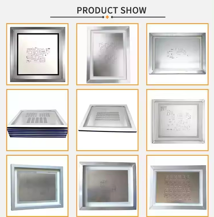
What is PCB stencil?
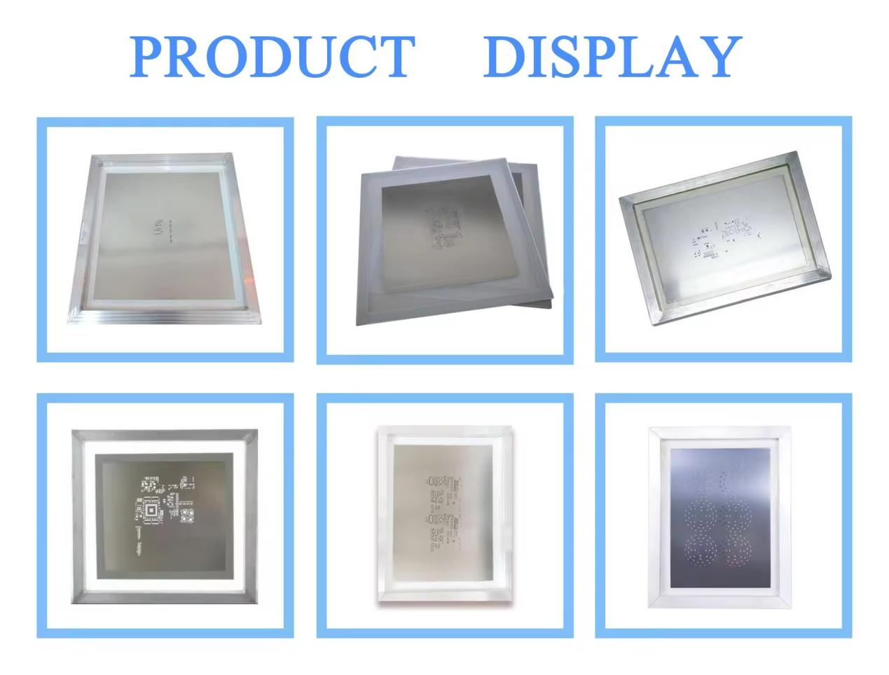
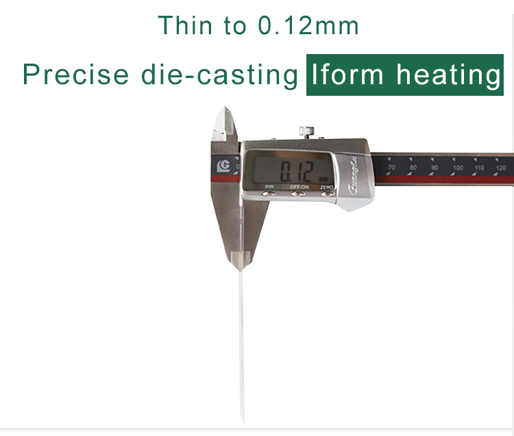
PCB Stencil is actually a very thin piece of steel. The size of the PCB Stencil is usually fixed to fit a paste printer. PCB Stencil is used from 0.08mm, 0.10mm, 0.12mm, 0.15mm, 0.18mm in thickness.
The stencil was originally made of wire mesh, so it was called a mask. It started with nylon polyester mesh, and later, due to its durability, it switched to wire mesh and copper wire mesh. Now it is stainless steel wire mesh. But no matter what material the wire mesh is made of, it has the disadvantage of bad shape and low precision. With the development of SMT technology, the requirement for SMT Stencil is higher and higher. SMT Stencil is coming into being. Stainless steel Stencil replaces them, which is now SMT Stencil.
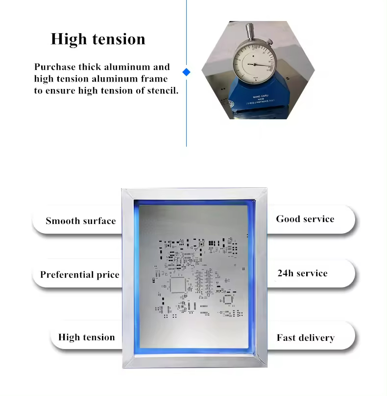
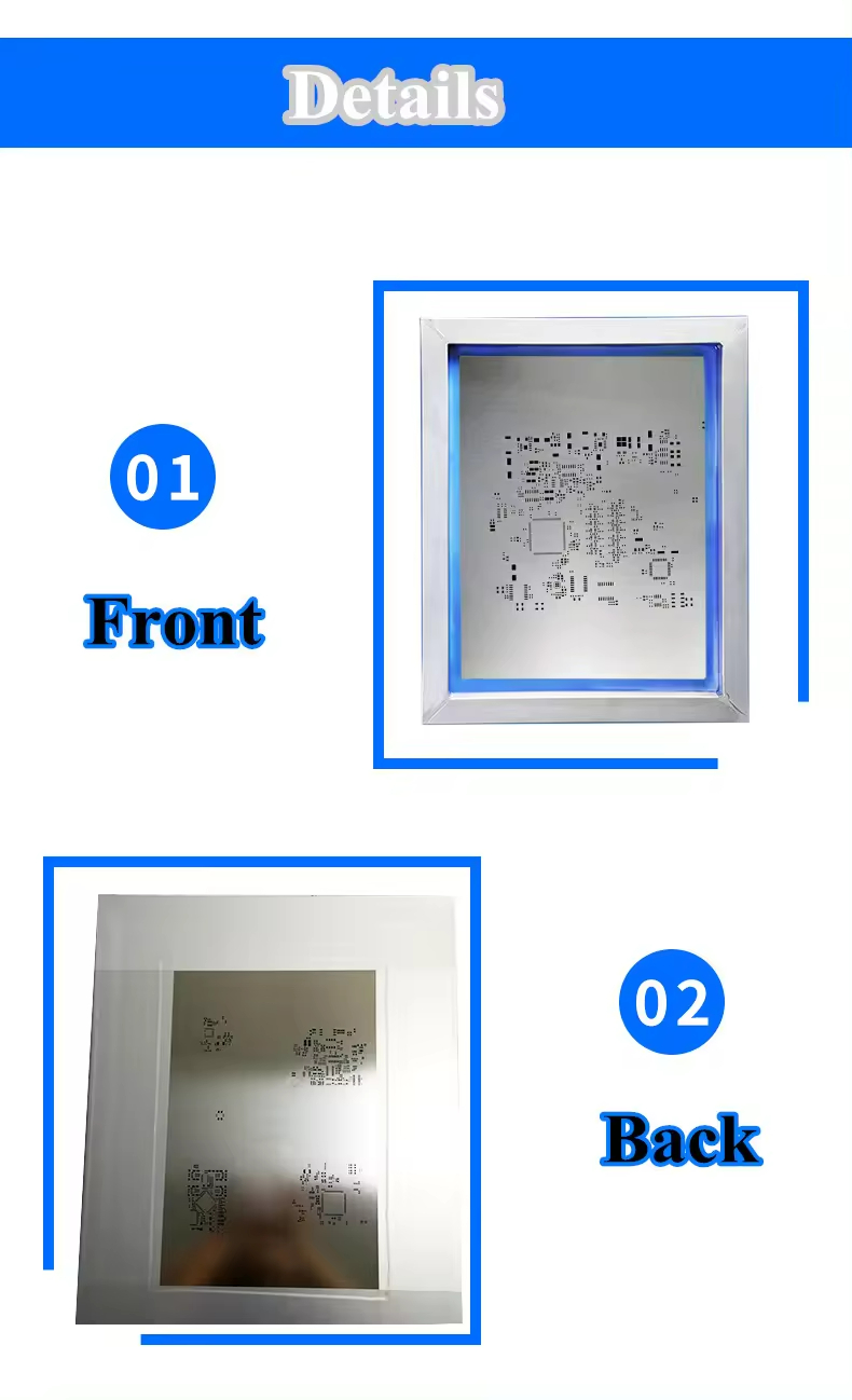
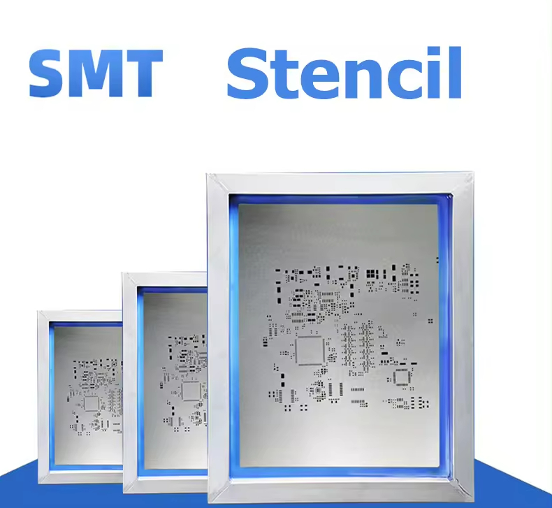
The main function of PCB Stencil is to assist in the deposition of solder paste and to transfer the exact amount of solder paste to the exact location on the bare PCB. PCB Stencil consists of a mesh frame, wire mesh, and steel sheet. There are many holes in the steel sheet, which correspond to the location on the PCB where printing is required. During use, place the PCB under the PCB Stencil and leak the paste onto the PCB through the holes in the fixed position on the PCB Stencil.
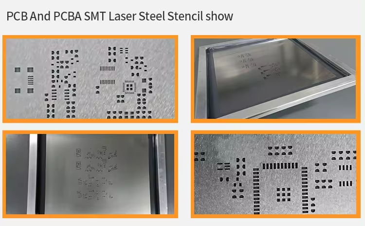
Pcb stencil produce capability:
Material | Foil: 304 stainless steel |
Frame: Aluminum | |
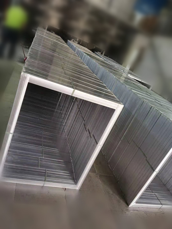
Stencil Size | 370x470mm [14.5’’x18.5’’] |
420x520mm [16.5’’x20.5’’] | |
550x650mm [22.0’’x25.5’’] | |
735x735mm [29.0’’x29.0’’] | |
Other size can be customized. | |
Long 1600mm SMT Stencil can be provided. | |
Stencil Type | SMT Stencil [Framed SMT Stencil] |
SMT Stencil Foil [Frameless SMT Stencil] | |
SS Foil Thickness | 0.10mm (4mil) |
0.12mm (5mil) | |
0.13mm (6mil) | |
0.15mm (7mil) | |
0.18mm (8mil) | |
0.20mm (10mil) |
PCB stencil is very important. In the process of PCB Assembly, the printing quality of PCB solder paste stencil will directly affect the processing quality of SMT, and the quality of solder paste printing is directly related to the quality of PCB stencil, so the correct design SMT stencil, the selection of the appropriate PCB stencil thickness and the design opening size of the PCB stencil, will be the key to ensuring the printing quality of the solder paste.
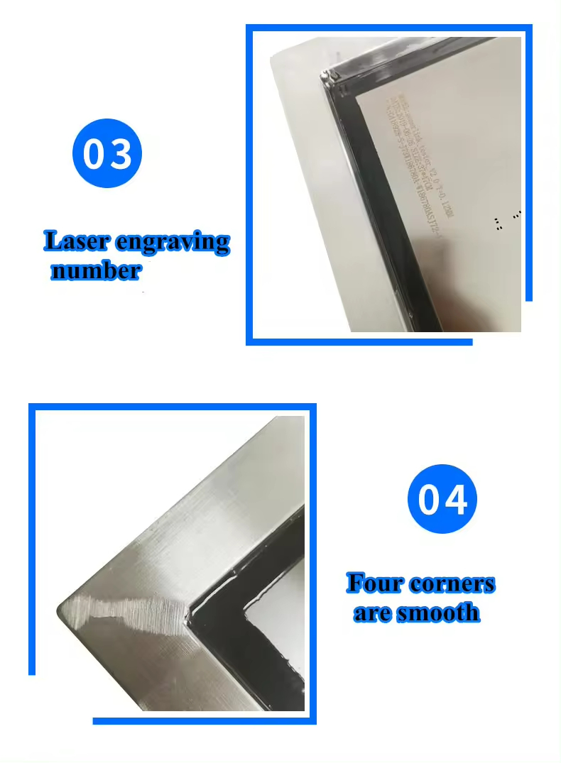
The key factors that affect the quality of PCB stencil are PCB stencil material and PCB stencil thickness, PCB stencil opening type, PCB stencil size, PCB stencil wall flatness. Therefore, in the PCB stencil design, Processing, inspection, and production process must pay special attention to PCB stencil.
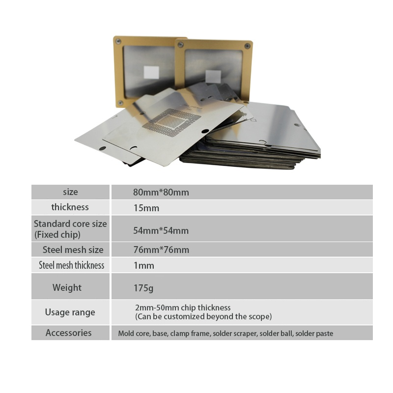
PCB stencil types
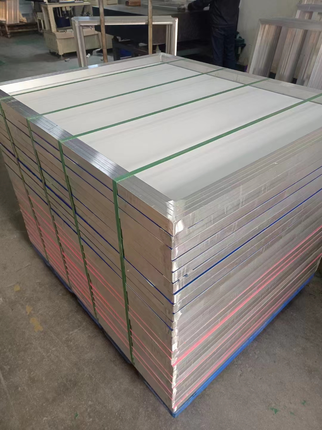
Framed PCB stencils are mostly ready to use. Framed stencil consists of a normal laser cut stencil sheet stained to the metal frame. This type of stencil is most suitable for high-volume SMT assembly due to the frame's ability to provide better stability and reusability of the stencil itself.
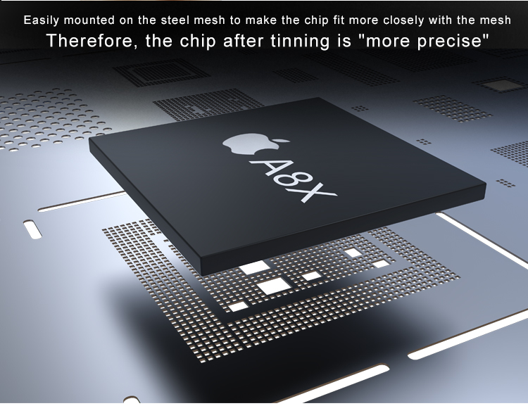
Frame of the stencil also allows a better and faster process of alignment between the PCB and stencil.Cost of the frame stencil is relatively higher due to the need for additional frame support . Moreover, frameworks require additional storage space and can be more complex to manage. It also makes stencil heavier, increasing shipping costs.
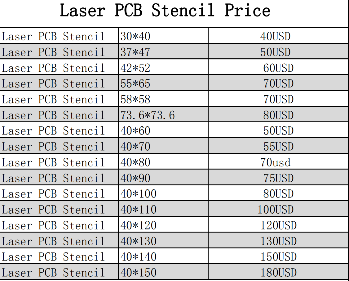
Stencil regular Specification and Price:
Unlike framed stencils, frameless stencils do not have a surrounding frame, making them more economical than framed stencils. This design allows for the direct placement of the stencil onto the PCB and it’s mostly suitable for hobby and non repeatable usage. Frameless stencils are very light which makes them great for shipping.
Due to no additional frame support being required, it is more suitable for small batch PCB printing and allows for custom sizes.Like framed stencils, frameless stencils can be customized to accommodate specific PCB designs and component layouts.
There are various components on the PCB, and each component has different solder paste requirements during the soldering process. Regular laser stencils can only regulate the amount of solder paste by adjusting the size of the openings while overall thickness of the stencil is the same everywhere.
Laser stencils use laser cut stencils. In recent years, laser stencil technology has developed rapidly, and laser stencil materials have been continuously updated. There are more and more laser cut stencils suppliers, and it is more and more convenient for customers to custom laser cut stencils.
How to select SMT Stencil?
1. Required minimum spacing and hole size.
2. The release paste performance of the template.
3. Reduce and prevent bridging, short circuits, or tin shortages of solder paste.
4. Cost, yield, and the cycle of processing materials.
5. The lifetime and durability of the template material.
6. Required solder paste thickness.
How to make PCB stencil?
Laser Stencil
Laser Stencil is currently the most commonly used template in the SMT Stencil industry. Laser Stencil features:
Direct use of data files to make, reduce the production error link; SMT Template Opening Position Accuracy is Extremely High: Whole Range Error < 4 μ M; The opening of the SMT template has a geometry which facilitates the printing of the solder paste.
PCB and data files are required to make laser Stencil.
PCB data must be edited correctly without distortion, damage, or fracture.
The acceptable data files for kx include GERBER, HPGL, JOB, PCB, GWK, CWK, PWK, DXF, PDF, PAD2000, POWER PCB, GCCAM4, PROTEL, AUTOCADR14 (2000), CLIENT98, CAW350W, V2001. The data must contain SMT solder paste layer as well as character layer data to check for positive and negative sides of the data, component categories, and so on.
Process flow of laser cutting Stencil, Filin making PCB_taking coordinates_data file_data processing_laser cutting_grinding_nets
Las Stencil features: high accuracy of data production, the small impact of objective factors; Trapezoid opening is good for demoulding; Can do precision cutting; The price is moderate.
Disadvantages of laser Stencil: Cutting one by one makes it slower.
Etching stencil
kx uses 301 steel sheets to make stencils. Etched Stencil is suitable for PCB board printing with angular position and spacing greater than or equal to 0.4MM. It is suitable for use with sheet copying and film. It can also use CAD/CAM and exposure mode simultaneously. Depending on the different parts, it can be scaled without calculating the price according to the number of parts. Etching stencils take a fast time to make. Etched PCB stencils are cheaper than laser stencils.
Process flow of chemical etch stencil: data file PCB_filming_exposure_development_etching_steel cleaning_wire mesh
Features: chemical etch stencil is formed at one time with a faster speed; Cheapness.
Disadvantages: chemical etch stencils tend to form hourglass shapes (not etched enough) or larger opening sizes (overstretched); The objective factors (experience, pharmaceuticals, film) have great influence, more production links, and large accumulative errors, which are not suitable for fine pitch Stencil production method. The preparation process is polluting the environment.
How to use PCB stencil?
1. PCB samples or PCB batches will become bare PCB boards. Next, we need to welding circuit board.
2. Cover the PCB steel mesh onto the PCB.
3. Print the solder paste on the surface of the PCB optical disc by SMT laser stencil.
4. Print the solder paste and mount the SMT device.
5. The pasted PCB is soldered by reflux soldering-overheating oven-semi-solid solder paste.
6. Bare PCB boards are now semi-finished PCBA products.
Things to note when using pcb stencil
1. Handle lightly;
2. Wash (wipe) Stencil before use to remove dirt carried during transportation;
3. Stir the paste or red glue evenly to avoid blocking the openings;
4. Optimal printing pressure: best pressure when the scraper just scrapes out the paste (red gel) on the Stencil;
5. It is best to use sticker printing when printing.
6. When the scraper has finished its journey, it is best to stop for 2-3 seconds before demolding, if possible, and the molding speed should not be too fast.
7. Do not hit PCB Stencil with hard objects or sharp knives;
8. Clean PCB Stencil after use and return to the box and place it on a special storage rack.
SMT stencil prices are calculated mainly by the following requirements:
1. Opening process, including etching, laser, ionic cascade, depends on the accuracy of the stencil opening and the product's process requirements. The cheapest and least accurate etching is also the lowest. Laser cutting of stencil is generally required for spacing less than 0.35.
2. Stencil thickness, different stencil thickness price is also different, in addition to the thickness process with special requirements, such as chemical staircase stencil price is higher.
3. Size, of course, the larger the size, the more expensive it is.
4. Material, Stencil border thickness dimensions, protective coating, etc.
5. Other requirements, such as single-sided network, double-sided network, and so on, vary in price.
The manufacturing process of PCB stencil has a great influence on the printing quality of the solder paste. Which PCB stencil to use depends on the product characteristics, size of welded terminals, component type, and component distribution of components on the PCB board.