Time:2024-06-24 Preview:200
High Frequency (HF) PCB Capability
What’s High Frequency (HF) PCB?
Applications of High Frequency PCB
How to Select PCB Materials for High Frequency Applications?
Materials Used for High Frequency Circuit Boards
High Frequency (HF) PCB Capability
Items | Manufacturing Capabilities | Remarks |
Number of Layers | 1-10 layers | For orders above 10 layers,please view the below "Standard PCB" or contact our sales rep. |
Material | FR-4,Aluminum | For Flex, Rigid-flex, Metal-based (Aluminum etc.,), HDI, Halogen-free, High Tg, etc.,please view the below "Standard PCB" or contact sales rep. |
Maximum PCB Size(Dimension) | 500*1100mm (min 5*6mm) | Any sizes beyond this dimension, please view the below "Standard PCB" or contact sales rep. |
Board Size Tolerance(Outline) | ±0.2mm/±0.5mm | ±0.2mm for CNC routing, and ±0.5mm for V-scoring. |
Board Thickness | 0.2-2.4mm | 0.2,0.4, 0.6, 0.8, 1.0, 1.2, 1.6, 2.0, 2.4mm. Please view the below "Standard PCB" or contact us if your board exceeds these. |
Board Thickness Tolerance(t≥1.0mm) | ±10% | Normally “+ Tolerance” will occur due to PCB processing steps such as electroless copper, solder mask and other types of finish on the surface. |
Board Thickness Tolerance(t<1.0mm) | ±0.1mm | |
Min Trace | 0.1mm/4mil | Min manufacturable trace is 4mil(0.1mm), strongly suggest to design trace above 6mil(0.15mm) to save cost. |
Min Spacing | Min manufacturable spacing is 4mil(0.1mm), strongly suggest to design spacing above 6mil(0.15mm) to save cost. | |
Outer Layer Copper Thickness | 1oz/2oz/3oz(35μm/70μm/105μm) | Also known as copper weight. 35μm=1oz, 70μm=2oz, 105μm=3oz. Please view the below "Standard PCB" or contact us if you need copper weight greater than 3oz. |
Inner Layer Copper Thickness | 1oz/1.5oz(35μm/50μm) | Inner copper weight as per customer’s request for 4 and 6 layers(Multi-layer laminated structure). Please contact us if you need copper weight greater than 1.5oz. |
Drill Sizes (CNC) | 0.2-6.3mm | Min drill size is 0.2mm, max drill is 6.3mm. Any holes greater than 6.3mm or smaller than 0.3mm will be subject to extra charges. |
Min Width of Annular Ring | 0.15mm(6mil) | For pads with vias in the middle, Min width for Annular Ring is 0.15mm(6mil). |
Finished Hole Diameter (CNC) | 0.2mm-6.2mm | The finished hole diameter will be smaller than size of drill bits because of copper plating in the hole barrels |
Finished Hole Size Tolerance(CNC) | ±0.08mm | For example, if the drill size is 0.6mm, the finished hole diameter ranges from 0.52mm to 0.68mm will be considered acceptable. |
Solder Mask | LPI | Liquid Photo-Imageable is the mostly adopted. Thermosetting Ink is used in the inexpensive paper-based boards. |
Minimum Character Width(Legend) | 0.15mm | Characters of less than 0.15mm wide will be too narrow to be identifiable. |
Minimum Character Height (Legend) | 0.8mm | Characters of less than 0.8mm high will be too small to be recognizable. |
Character Width to Height Ratio (Legend) | 1:05 | In PCB silkscreen legends processing, 1:5 is the most suitable ratio |
Minimum Diameter of Plated Half Holes | 0.6mm | Design Half-Holes greater than 0.6mm to ensure better connection between boards. |
Surface Finishing | HASL with lead | The most popular three types of PCB surface finish. Please view the below "Standard PCB" or contact us for other finishes. |
HASL lead free | ||
Immersion gold,OSP | ||
Solder Mask | Green ,Red, Yellow, Blue, White ,Black | No extra charge (Green, Red, Yellow, Blue) |
Silkscreen | White, Black, None | No extra charge. |
Panelization | V-scoring, | Leave min clearance of 1.6mm between boards for break-routing. For V-score panelization, set the space between boards to be zero. |
Tab-routing, | ||
Tab-routing with Perforation (Stamp Holes) | ||
Others | Fly Probe Testing (Free) and A.O.I. testing(free), ISO 9001:2008 ,UL Certificate | No extra charge. |

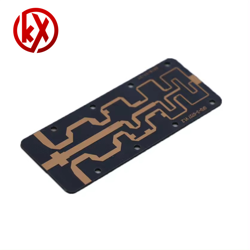
High Frequency (HF) PCB is used to transmit electromagnetic waves in the frequency of GHz with minimal loses in the variety of applications, including mobile, microwave, radio frequency (RF) and high-speed design applications. Hence, printed circuit boards with some specific characteristics are used to transmit these electromagnetic waves. Several parameters are taken into considerations while designing a PCB for high frequency applications.
A high frequency PCB can meet your needs when incorporating a special signal requirement into your electronic devices and products. These higher transmission frequencies are capable of supporting the faster signal flow rates that are a necessity in today’s increasingly complex electronic switches and other components.
The increasing complexity of electronic components and switches continually requires faster signal flow rates, and thus higher transmission frequencies. Because of short pulse rising times in electronic components, it has also become necessary for high frequency technology to treat conductor widths as an electronic component. Depending on various parameters, high frequency signals are reflected on printed circuit board, meaning that the impedance varies with parameters must be exactly specified, and implemented with the highest level of process control.

High frequency PCBs are always used in the following applications
· Automotive Radar Systems
· Global Positioning Satellite Antennas
· Cellular Telecommunications Systems – Power Amplifiers and Antennas
· Direct Broadcast Satellites
· E-band Point to Point Microwave Links
· RF Identification (RFID) Tags
· Airborne and Ground Based Radar Systems
· Millimeter Wave Applications
· Missile Guidance Systems
· Space Satellite Transceivers
The demand for high frequency printed circuit board is on the rise in the various industrial vectors. They meet the requirements which traditional PCB fail to deliver efficiently. If you are still skeptical about incorporating high frequency PCBs in your electronics, you can always approach an industry expert in kx PCB. The company has provided standard, as well as customized high frequency circuit boards to various industries.

The PCB laminate materials you select for your PCB building can be critically important to the overall functionality and lifespan of your final product. When operating frequencies go into the Microwave or even Radio Frequency (RF) regions, your PCB laminate material selection will have a significant impact on the overall loss of the finished PCB after PCB assembly and final assembly. Electrical, thermal, and mechanical properties must all be considered carefully when determining the best suitable material for your high frequency PCB manufacturing.
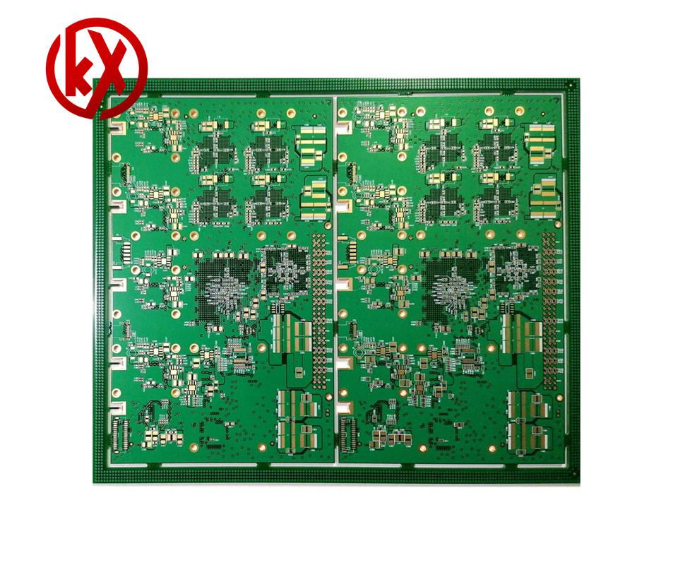
In high frequency designs, you may find that FR4 sometimes just doesn’t to do the job at some higher frequencies. It’s obvious you select a wrong PCB material. The main concern with FR4 at high frequencies is its relatively high dielectric constant (Dk), which is typically considered to be approximately 4.2. While, FR4 can still act as a suitable laminate material for high frequency PCBs when it comes to a hybrid construction, in which the fabrication is combined with high frequency laminate. At kxPCB, we carry a selection of materials specifically designed to maintain signal integrity in Radio Frequency and Microwave regions.
High-frequency boards have special demands on the material used:
· Adapted dielectric permittivity
· Low attenuation for efficient signal transmission
· Homogeneous construction with low tolerances in insulation thickness and dielectric constant
For may applications, it is sufficient to use FR-4 material with an appropriate layer buildup. In addition, we process high frequency materials with improved dielectric properties. These have a very low loss factor (Df), a low dielectric constant, and are primarily temperature and frequency independent.
Additional favorable properties are high glass transition temperature (Tg), an excellent thermal durability, and very low hydrophilic rate.
We use PTFE materials for impedance controlled high frequency printed circuit boards. Sandwich buildups for material combinations (hybrid structures) are also possible.
Material for HF PCBs | Dk (@10GHz) | Df (@10GHz) | Tg (°C) | Td (°C) | Z CTE (ppm/°C) | Surface Resistivity (MΩ) | Thermal Conductivity (W/m·K) | Peel Strength (N/mm) |
Rogers RO4003C (Reinforced Hydrocarbon/Ceramic) | 3.38 | 0.0027 | >280 | 425 | 46 | 4.2 x 10⁹ | 0.71 | 1.05 |
Rogers RO4350B (Reinforced Hydrocarbon/Ceramic) | 3.48 | 0.0037 | >280 | 390 | 32 | 5.7 x 10⁹ | 0.69 | 0.88 |
RT/duriod 5870 (Reinforced PTFE) | 2.33 | 0.0012 | – | 500 | 173 | 2 x 10⁷ | 0.22 | 27.2 |
RT/duroid 5880 (Reinforced PTFE) | 2.2 | 0.0009 | – | 500 | 237 | 3 x 10⁷ | 0.2 | 31.2 |
Rogers RO3003 (Ceramic-filled PTFE) | 3 | 0.0013 | – | 500 | 25 | 1 x 10⁷ | 0.5 | 2.2 |
Rogers RO3006 (Ceramic-filled PTFE) | 6.2 | 0.0020 | – | 500 | 24 | 1 x 10⁵ | 0.79 | 1.2 |
Rogers RO3010 (Ceramic-filled PTFE) | 10 | 0.0022 | – | 500 | 16 | 1 x 10⁵ | 0.95 | 1.6 |
isola IS620 (E-fibre glass) | 4.5* | 0.0080 | 220 | – | 55 | 2.8 x 10⁶ | – | 1.2 |
AGC Taconic RF-35 (Ceramic) | 3.5** | 0.0018 | 315 | – | 64 | 1.5 x 10⁸ | 0.24 | 1.8 |
AGC Taconic TLX (PTFE) | 2.5 | 0.0019 | – | – | 135 | 1 x 10⁷ | 0.19 | 2.1 |
AGC Taconic TLC (PTFE) | 3.2 | – | – | – | 70 | 1 x 10⁷ | 0.24 | 2.1 |
ARLON 85N (Polyimide) | 4.2* | 0.0100 | 250 | 387 | 55 | 1.6 x 10⁹ | 0.2 | 1.2 |
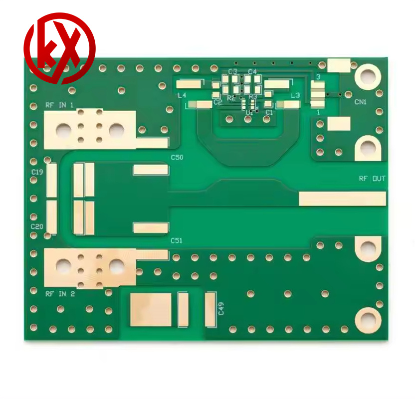 At KXPCB, we normally keep stock of these high frequency PCB laminates, like Rogers PCB, since these are the most commonly requested. But it is always a good idea to contact kxPCB in advance for ensuring we have the specific HF material required in your new project.
