Time:2024-03-01 Preview:109
Deformation caused during PCB board processing
The causes of printed circuit board deformation during processing are very complex and can be divided into two types of stress: thermal stress and mechanical stress.
Thermal stress is mainly generated during the lamination process, and mechanical stress is mainly generated during the stacking, pcb assembly,printed circuit board assembly,pcba handling,circuit board assembly and baking processes of panels. The following is a brief discussion in process order.

1. Causes of PCB warping
The main reasons for PCB warpage are as follows:
First, the weight and size of the circuit board itself are too large, and the support points are located on both sides, which cannot effectively support the entire board, resulting in depression and deformation in the middle.
Secondly, the V-cut is too deep, causing the V-cuts on both sides to warp. V-Cut cuts grooves in the original large sheet, so it is easy for the board to warp.
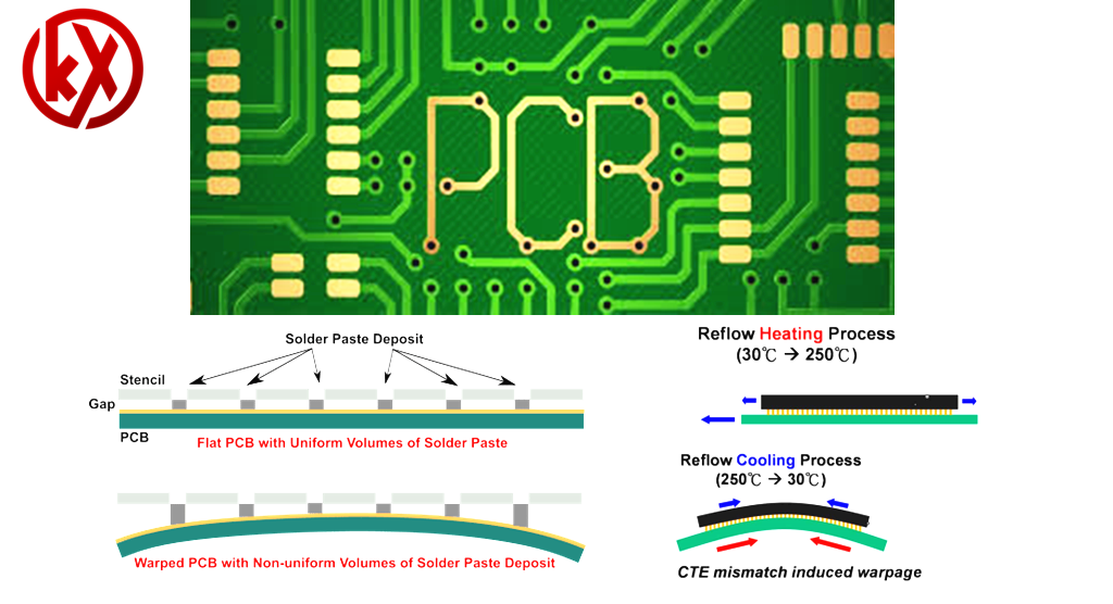
In addition, the material, structure, and graphics of PCB will have an impact on board warpage. pcb circuit is made of core board, prepreg and outer copper foil. The core board and copper foil will be deformed by heat when pressed together. The amount of warpage depends on the coefficient of thermal expansion (CTE) of the two materials.
2. Warpage caused during PCB processing
The reasons for printing circuit boards processing warpage are complex and can be divided into thermal stress and mechanical stress. Among them, thermal stress is mainly generated during the pressing process, and mechanical stress is mainly generated during the stacking, handling and baking processes of the plates.
1. In the process of incoming copper clad laminates, since the copper clad laminates are double-sided, symmetrical in structure, and without graphics, the CTE of copper foil and glass cloth are almost the same, so there is almost no warpage caused by different CTE during the pressing process. However, during the pressing process, due to the large size of the press, the temperature difference in different areas of the hot plate will cause slight differences in the resin curing speed and degree of curing in different areas during the pressing process. At the same time, the dynamic viscosity at different heating rates is also greatly different, so local stress will also be generated due to different curing processes. Generally, this stress will remain balanced after pressing, but will gradually release and deform during subsequent processing.
2. During the PCB pressing process, due to the thicker thickness, diverse pattern distribution, and more prepregs, thermal stress will be more difficult to eliminate than copper-clad boards. The stress in the PCB board is released during the subsequent drilling, forming or baking process, causing the board to deform.
3. During the solder mask and silk screen baking process, since the solder mask inks cannot stack on each other during the curing process, thepcb manufacturing will be placed in the rack to bake the board for solidification. The solder resist temperature is around 150°C, which exceeds the Tg value of the copper-clad board. The PCB is prone to softening and cannot withstand high temperatures. Therefore, manufacturers must heat both sides of the substrate evenly while keeping the processing time as short as possible to reduce substrate warpage.
4. During the cooling and heating process of PCB, thermal stress will be generated due to the inhomogeneity of material properties and structure, resulting in microscopic strain and overall deformation and warping. The tin furnace temperature range is 225℃ to 265℃, the hot air solder leveling time for ordinary boards is between 3 seconds and 6 seconds, and the hot air temperature is 280℃ to 300℃. After the solder is leveled, the board is put into the tin furnace from a normal temperature state and washed with normal temperature post-processing water within two minutes after coming out of the furnace. The entire hot air soldering leveling process is a rapid heating and cooling process. Due to the differences in circuit board materials and structural inhomogeneity, thermal stress will inevitably occur during the cooling and heating processes, resulting in microscopic strain and overall deformation and warping.
5. Improper storage conditions can also cause PCB warping.
PCB boards are generally stored vertically in racks during the semi-finished product stage. Improper adjustment of the rack's tightness or stacking of boards during storage will cause mechanical deformation of the boards. Especially for thin plates below 2.0mm, the impact is more serious.
6.Pcb board design reasons:
1. If the copper surface area on the circuit board design is uneven, one side is larger and the other side is smaller, the surface tension will be weaker where the lines are sparse than where they are dense, which may cause the board to warp when the temperature is too high.
2. Special dielectric or impedance relationships may cause the laminate structure to be asymmetrical, resulting in board warping.
3. If the printed circuit board design itself has large and large number of hollows, it is easy to warp when the temperature is too high.
In addition to the above factors, there are many factors that affect PCB board deformation.The condition make pcb board manufacturer,printed circuit board manufacturers,circuit board manufacturing,pcb board maker,very trouble, If you want to learn more,please contact sales@kxpcba.com