Time:2024-05-28 Preview:231
Flex PCB Assembly Capability:
Flexible PCB assembly process
Design considerations for flex PCB assembly
Flex PCB Classifications
Flex PCB Advantages
Flex Circuit Design Steps
Flex Circuit Design Rules
Characteristics of flex board assembly
Flex PCB assembly is the process of assembling components on a flex board. This assembly process is similar to that of rigid boards. Scroll down to learn more about this topic as we answer some of the most common questions.
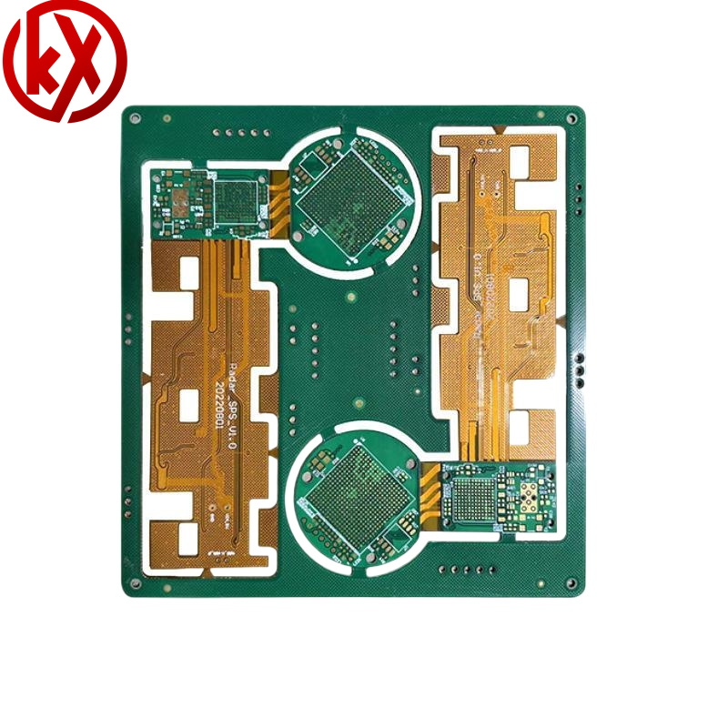
We are more than your PCB manufacturer. We help you flex your design potential. Get low-to-high volume flex and rigid-flex PCBs manufactured with industry leading quick turnaround times. Start building a quote online now.
Flex PCB Assembly Capability:
Item | Capability | |
1 | Single and double sided SMT/PTH | Yes |
2 | Large parts on both sides, BGA on both sides | Yes |
3 | Smallest Chips size | 0201 |
4 | Min BGA and Micro BGA pitch and ball counts | 0.008 in. (0.2mm) pitch, ball count greater than 1000 |
5 | Min Leaded parts pitch | 0.008 in. (0.2 mm) |
6 | Max Parts size assembly by machine | 2.2 in. x 2.2 in. x 0.6 in. |
7 | Assembly surface mount connectors | Yes |
8 | Odd form parts: LED Resistor and capacitor networks Electrolytic capacitors Variable resistors and capacitors (pots) Sockets | Yes |
9 | Wave soldering | Yes |
10 | Max PCB size | 14.5 in. x 19.5 in. |
11 | Min PCB Thickness | 0.02 |
12 | Fiducial Marks | Preferred but not required |
13 | PCB Finish: | 1.SMOBC/HASL 2.Electrolytic gold 3.Electroless gold 4.Electroless silver 5.Immersion gold 6.Immersion tin 7.OSP |
14 | PCB Shape | Any |
15 | Panelized PCB | 1.Tab routed 2.Breakaway tabs 3.V-Scored 4.Routed+ V scored |
16 | Inspection | 1.X-ray analysis 2.Microscope to 20X |
17 | Rework | 1.BGA removal and replacement station 2.SMT IR rework station 3.Thru-hole rework station |
18 | Min IC Pitch | 0.2mm |
19 | solder paster printer | 0.2mm |
20 | POP Manufacturing capability | POP *3F
|
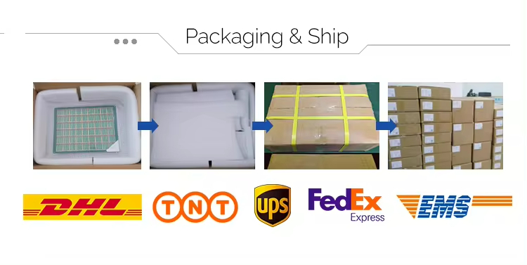
Flex board assembly is the process of assembling components. This process is similar to that of rigid boards. Below image shows the process flow.
BOM or bill of materials is a list of components required to assemble a printed circuit board.
A flex circuit board stack-up is set and sent to the baking process to reduce the amount of moisture inside the board. The temperature and duration of the baking process depends on the overall thickness of the PCB.
Overall thickness of flex PCB | Duration and temperature of baking |
Upto 1 mm (39 mils) | minimum 2 hours at 120 °C |
> 1 mm upto 1.8 mm (70 mils) | minimum 4 hours at 120 °C |
> 1.8 mm upto 4 mm (157 mils) | minimum 6 hours at 120 °C |
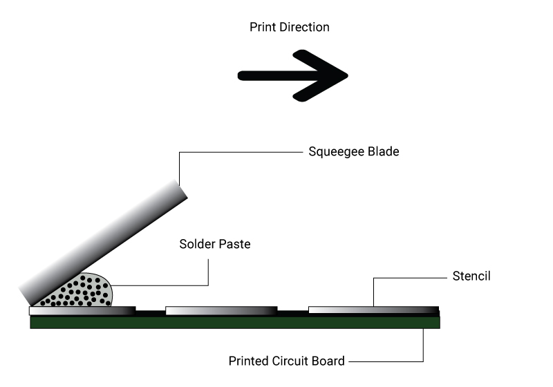
Post baking, the board undergoes solder paste printing. In this process solder paste is applied on the PCB surface. The primary goal here is to solder pads onto the circuit board. This is done by screen printing the solder paste through a stencil. A tool called squeegee blade is used to apply the required force on the solder paste to move it across the stencil. Squeegees are generally made of metal or polyurethane.
Silkscreen printing is a process of creating a layer of non conductive ink traces used to identify components, test points, parts of the circuit board, warning symbols, logos and marks, etc. This process is only performed if the customer has asked for it. Component mounting is performed after the silkscreen printing. After placing the components, the board is visually inspected and sent to the reflow soldering process.

Reflow soldering is a process of pre-heating the components and melting the solder on the PCB to accomplish solder joints between the board and the components. The components are glued to the flex board by the solder paste. This solder paste melts down during the reflow soldering process and cools down to create a good solder joint. This takes place in reflow ovens. These ovens have different heating zones. Each heating zone has its temperature set as per the solder profiles of the assembly process.
Reflow soldering has four stages:
In the preheat stage, heat is accumulated in the board and the components. The temperature should gradually change because quick changes in temperature can damage the components. Generally, the temperature change is no more than 2°C/second. This information can be found in the solder paste datasheet.
During the thermal soak stage, the oxidation of pads and leads of components are reduced by activating the flux.
In the reflow stage, the solder paste is melted and the process reaches its maximum temperature (lesser than the maximum allowed temperature of the components). The processed board is then cooled down and the solder alloy solidifies to create solder joints.
In the further stages, the flex board is optically inspected and electrically tested to ensure it is 100% error free. Post testing, it is punched out of the panel and sent to final quality check (FQC). After FQC the circuit board is sent to packaging and warehousing.
Important flex PCB assembly specifications that a designer needs to know.
1. Base materials: The most common base material used in flex boards is polyimide films. These materials are flexible and thin. Choose a material with good thermal resistance and electrical conductivity.
2. Number of layers: The number of layers in a flexible PCB depends on the type of application it is used in. For dynamic applications, opt a single layer board. For static, the number of layers can vary from 4 to 8.
3. Bend radius: The bend radius of a flex circuit determines the bendability of it. Generally, the bend radius of these boards vary between 1 mm and 5 mm.
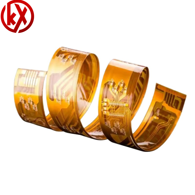
Flex PCBs can be easily bent without breaking.
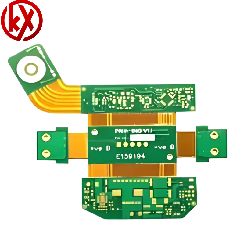
Flex PCBs can be classified into rigid-flex PCBs and high-density interconnect (HDI) rigid-flex PCBs.
The number of layers of flex PCBs vary between 1 and 6. It is preferable to limit the number of layers to a max of 2 for greater cost benefits and mechanical flexibility.
Flex circuit design rules are different from rigid PCB design rules
Whenever board design needs to be flexible and capable of withstanding vibrations, flex circuit design rules are applied by PCB designers. In addition to bendability and vibration resistance, flexible PCBs are helpful for saving space. Lightweight flex PCBs improve air circulation and thermal performance and reduce manufacturing costs.
Basically, there are two types of PCB boards based on their flexibility: rigid boards and flexible boards. For certain applications, installing a rigid PCB is tough. Bringing the rigid PCB to the exact position required might even become impossible when there are space constraints and access difficulties. In such circumstances, flexibility is required.
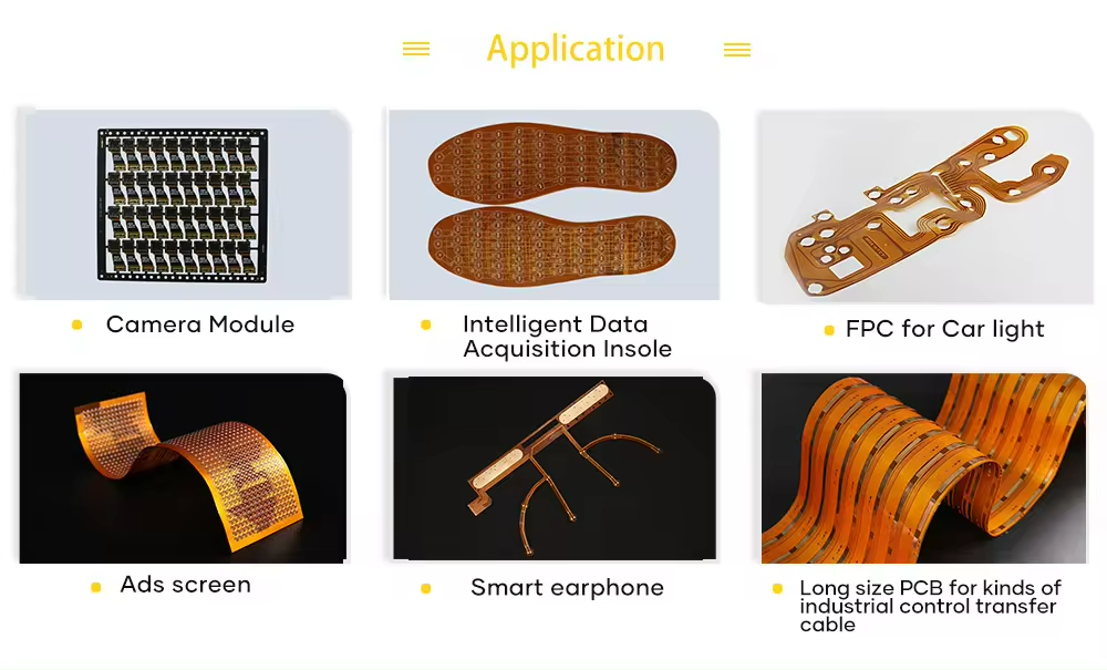
Flexible PCBs can be easily bent without breaking and are more easy to manuever into place. Flexible boards are made out of thin, flexible materials that offer high tensile strength. Usually, flexible PCBs are employed when electronic circuits are required in confined areas or movable sections of a product. They are preferred when designs are required to be lightweight and small while maintaining the same performance, efficiency, and reliability.
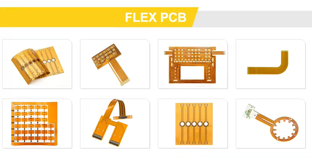
Flex PCBs can be classified into rigid-flex PCBs and high-density interconnect (HDI) rigid-flex PCBs.
Rigid-Flex PCBs | High-Density Interconnect Rigid-Flex PCBs |
When the PCB is made of both rigid and flexible materials, it forms rigid-flex PCBs. They are extremely bendable and foldable to any shape. | Characterized by closer spaces, a higher number of layers, and denser wiring. Offers faster connections at a reduced size. |
Improved Reliability | It is possible to customize the routing path. By doing so, the routing path becomes more dependable due to the reduction in integrity issues. Reliability can be enhanced with flex PCBs. |
Withstands High Temperatures and Vibrations | The circuits used in aerospace, avionics, medical, and military applications have to withstand high temperatures and vibrations. Circuits need to withstand high strain without breakage or loss of strength. Considering the temperature and vibration aspects, flex PCBs endure both and are ideal for harsh environments. |
Saves Costs and Space | As flex circuits cut down the amounts of wires and cables, this results in space saving and weight reduction. Flex circuits offer seamless integration of various designs into a single compact circuit. Assembly time and cost is therefore reduced. |
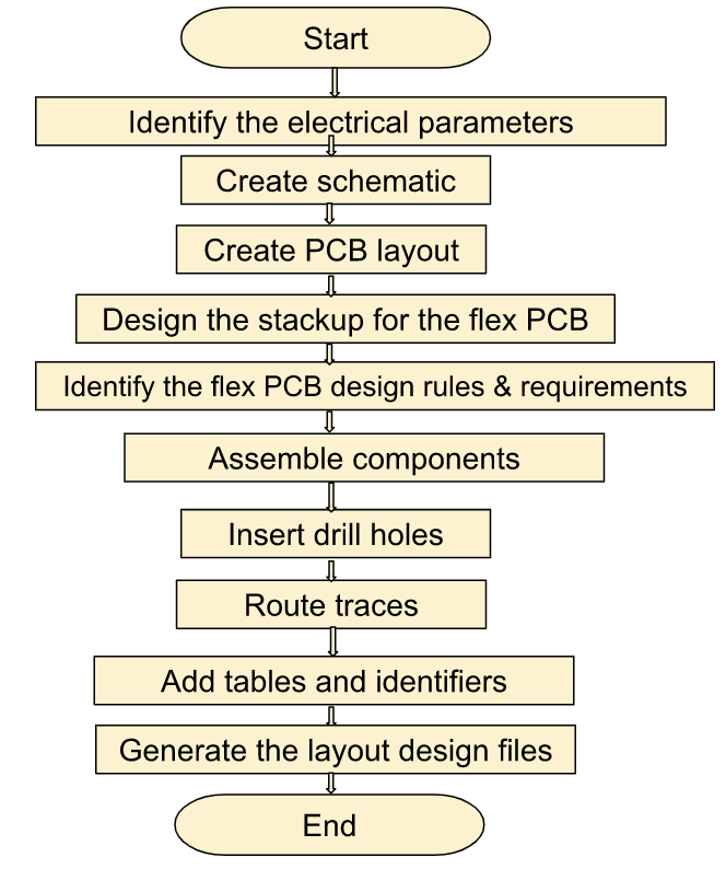
The following flow chart introduces the steps involved in designing a flex PCB.
1 | The number of layers of flex PCBs vary between 1 and 6. It is preferable to limit the number of layers to a max of 2 for greater cost benefits and mechanical flexibility. |
2 | Within the flexible area of the rigid-flex PCB, the trace width and spacing should be maintained as wide as possible. |
3 | The solder pads and tracks need to be connected in a round or teardrop-like shape. |
4 | Make the soldering surfaces and annular rings as large as possible. |
Flex boards are prone to wear and tear as they are thin and light weighted. To successfully assemble SMT components, rigid carriers are used. The positioning and consistency of the carrier plays a vital role in the assembly process. Lots of auxiliary fixtures are implemented in flex assembly, including board carrying tray, baking, electrical test, function test, and cutting fixtures.
The number of components that can be assembled on flex PCBs is relatively low when compared to rigid boards.
Generally, these boards are used in places where it requires repeated flexing. The components assembled have to meet the demands of their operating conditions. Therefore, flex circuit boards demand higher standards in terms of cleanliness and soldering reliability than rigid PCBs.
Compared to rigid PCB assembly, flex assembly expenses are higher with longer manufacturing duration. The process demands more accessories and staff, and requires a well maintained manufacturing environment.
